← Akaza (Top Project Slayers) – The Ultimate Character Guide! akaza top Arduino Mega 2560 Altium Library – Free Download for PCB Pros! arduino mega 2560 pcb layout proteus →
If you are searching about Designing PCIe interfaces and extenders « Adafruit Industries – Makers you've visit to the right place. We have 25 Images about Designing PCIe interfaces and extenders « Adafruit Industries – Makers like PCI and PCIe in PCB Layout Design-ELEPCB - ELEPCB, PCIE-PCB设计规范!(建议收藏)-CSDN博客 and also Review of Server PCB Layout & Schematic - Part 4: PCI Express (PCIE. Here it is:
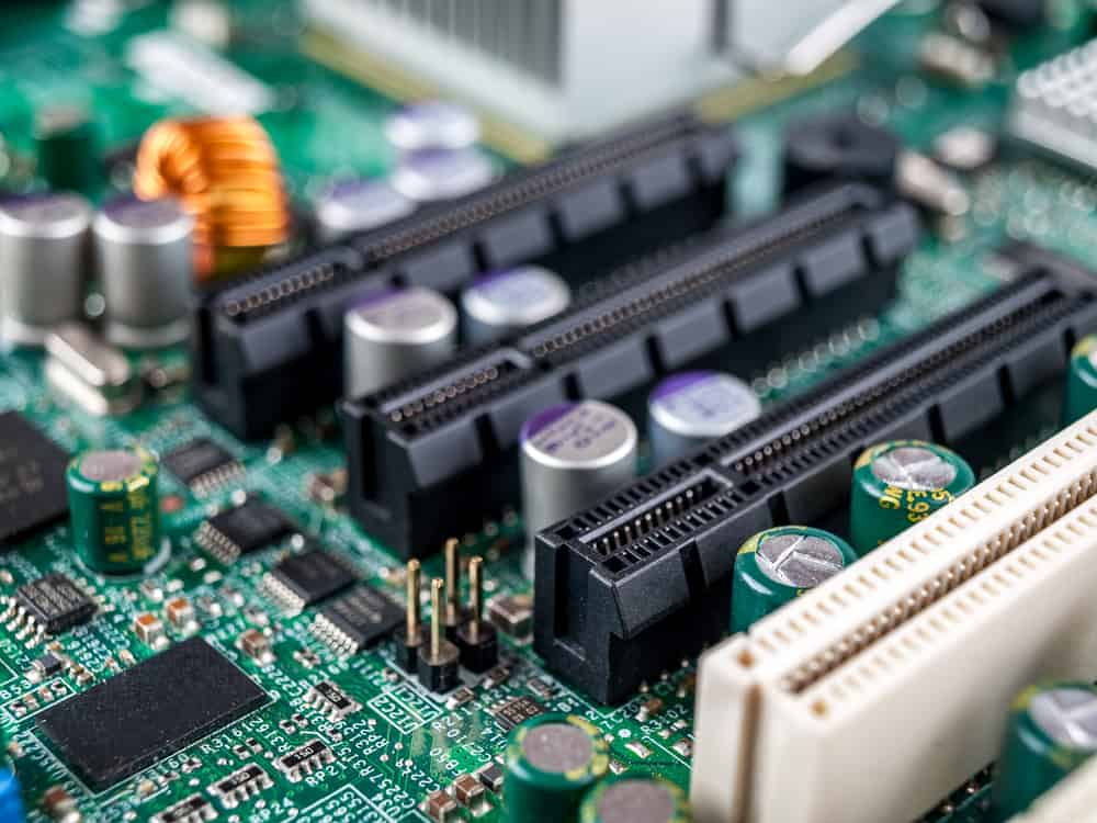
Designing PCIe Interfaces And Extenders « Adafruit Industries – Makers
 blog.adafruit.com
Designing PCIe interfaces and extenders « Adafruit Industries – Makers ...
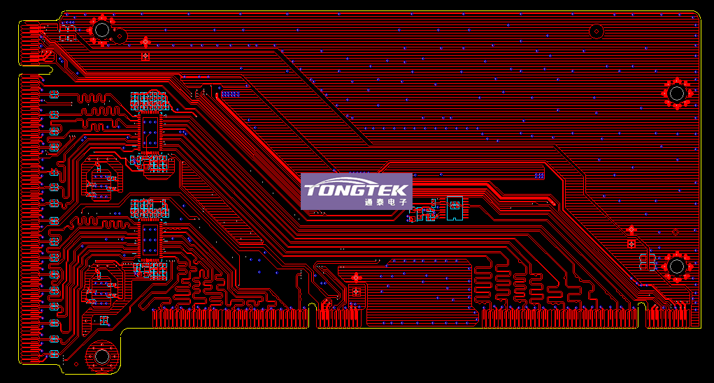
PCIE转接板 - PCB设计案例 - 通泰电子
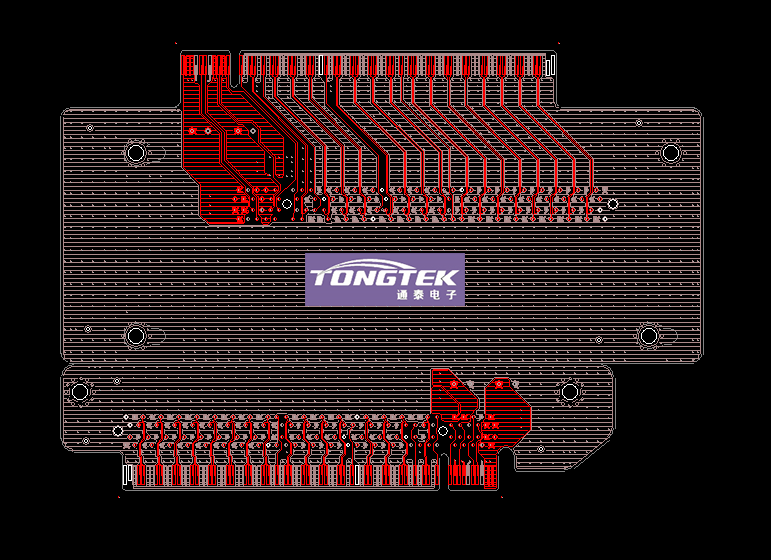 www.tontektech.com
PCIE转接板 - PCB设计案例 - 通泰电子
PCI Express: PCIe PCB Manufacturing, Assembly, Design | MADPCB
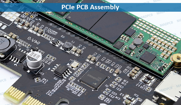 madpcb.com
PCI Express: PCIe PCB Manufacturing, Assembly, Design | MADPCB
PCI Express PCB Layout Guidelines - PCBBUY.COM
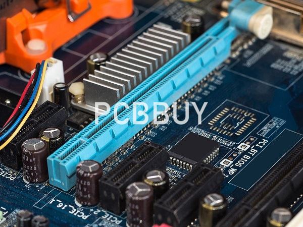 www.pcbbuy.com
PCI Express PCB Layout Guidelines - PCBBUY.COM
PCIe In PCB Design: Layout And Routing Guidelines | Blog | Altium Designer
PCIe in PCB Design: Layout and Routing Guidelines | Blog | Altium Designer
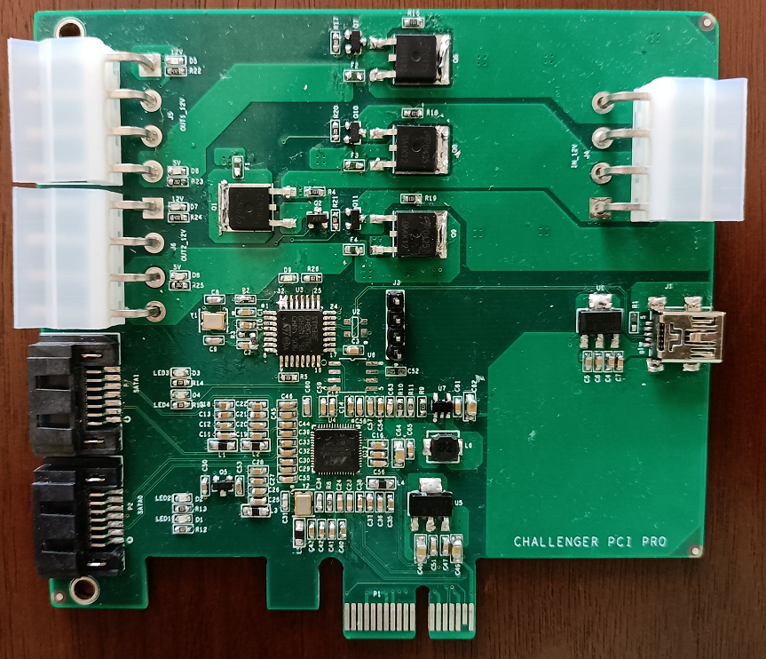
PCIE转接板 - PCB设计案例 - 通泰电子
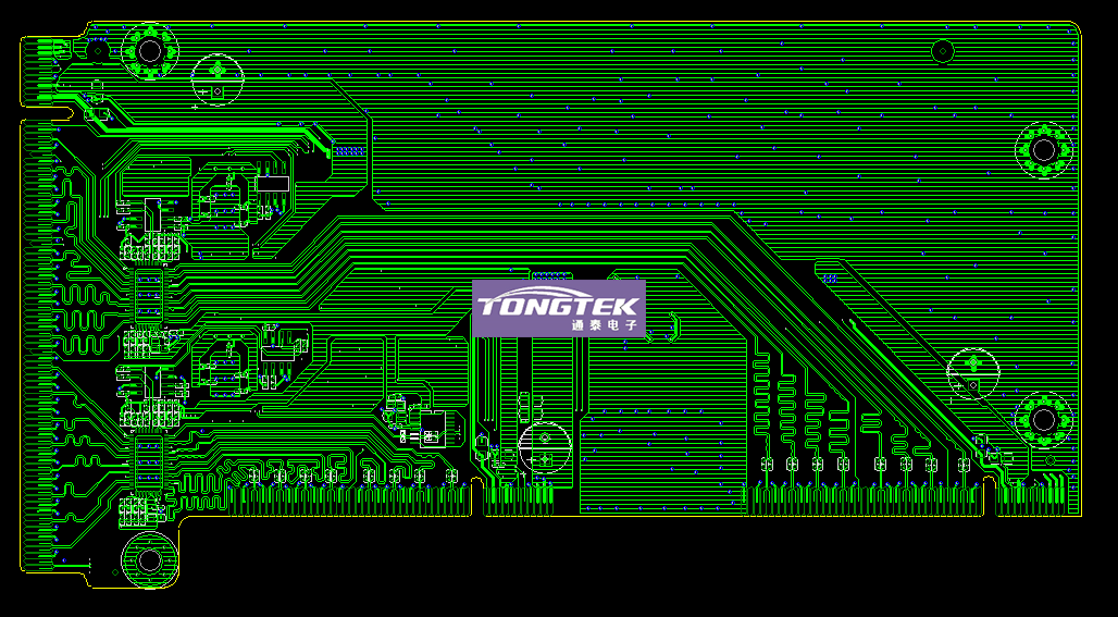 www.tontektech.com
PCIE转接板 - PCB设计案例 - 通泰电子
PCIe Routing Guidelines & Best Practices - Free Online PCB CAD Library
 www.ultralibrarian.com
PCIe Routing Guidelines & Best Practices - Free Online PCB CAD Library
PCIe In PCB Design: Layout And Routing Guidelines | Blog | Altium Designer
 resources.altium.com
PCIe in PCB Design: Layout and Routing Guidelines | Blog | Altium Designer
PCIE-PCB设计规范!(建议收藏)-CSDN博客
PCIE-PCB设计规范!(建议收藏)-CSDN博客
Review Of Server PCB Layout & Schematic - Part 4: PCI Express (PCIE
 www.youtube.com
Review of Server PCB Layout & Schematic - Part 4: PCI Express (PCIE ...
PCIe Routing Guidelines & Best Practices - Free Online PCB CAD Library
 www.ultralibrarian.com
PCIe Routing Guidelines & Best Practices - Free Online PCB CAD Library
PCIe In PCB Design: Layout And Routing Guidelines | Blog | Altium Designer
PCIe in PCB Design: Layout and Routing Guidelines | Blog | Altium Designer
PCB Layout Guidelines For High Speed Applications - HardwareBee
 hardwarebee.com
PCB Layout Guidelines For High Speed Applications - HardwareBee
PCB Routing Guidelines - Part 12 (PCIe Signals)
 embeddeddesignblog.blogspot.com
PCB Routing Guidelines - Part 12 (PCIe signals)
Impedance Matching - PCB Design For High-frequency Differential Lanes
 electronics.stackexchange.com
impedance matching - PCB design for high-frequency differential lanes ...
Pcb - PCIe High Speed Signal TX And RX Routing With Via - Electrical
 electronics.stackexchange.com
pcb - PCIe high speed signal TX and RX routing with via - Electrical ...
PCB Layout Guidelines | Design Rules & Requirements | Tips
 www.wellpcb.com
PCB Layout Guidelines | Design Rules & Requirements | Tips
PCIE-PCB设计规范!(建议收藏)-CSDN博客
PCIE-PCB设计规范!(建议收藏)-CSDN博客
PCI And PCIe In PCB Layout Design-ELEPCB - ELEPCB
 www.elepcb.com
PCI and PCIe in PCB Layout Design-ELEPCB - ELEPCB
PCIE转接板 - PCB设计案例 - 通泰电子
 www.tontektech.com
PCIE转接板 - PCB设计案例 - 通泰电子
PC & PCI Cards - Multi Circuit Boards
 www.multi-circuit-boards.eu
PC & PCI cards - Multi Circuit Boards
PCIe Standard For PCB Design. – PCBSky
 www.pcbsky.com
PCIe standard for PCB design. – PCBSky
BRAINE_PCIe - PCB Design
 pcbdesign.hu
BRAINE_PCIe - PCB Design
PCI And PCIe In PCB Layout Design-ELEPCB - ELEPCB
 www.elepcb.com
PCI and PCIe in PCB Layout Design-ELEPCB - ELEPCB
Rolling Your Own PCIe Bifurcation Riser – Matt's Tech Pages
 www.mattmillman.com
Rolling your own PCIe Bifurcation riser – Matt's Tech Pages
pci express pcb layout guidelines. Pcb layout guidelines. Pci and pcie in pcb layout design-elepcb